University of Sussex physicists have created an extremely thin, large-area terahertz semiconductor surface source made of just a few atomic layers and compatible with existing electronic platforms.
Terahertz sources produce brief light pulses that oscillate at a trillion times per second. At this scale, they are too fast for standard electronics and, until recently, too slow for optical technologies. This has significant implications for the evolution of ultra-fast communication devices above the 300GHz limit, such as those required for 6G mobile phone technology, which is still fundamentally beyond the capabilities of current electronics.
Researchers at Sussex’s Emergent Photonics (EPic) Lab, led by Director of the Emergent Photonics (EPic) Lab Professor Marco Peccianti, are pioneers in surface terahertz emission technology, having demonstrated the brightest and thinnest surface semiconductor sources to date. Their new development, a terahertz semiconductor source, has an emission region that is 10 times thinner than previously achieved, with comparable or even better performance.
Physicists have developed an extremely thin, large-area semiconductor surface source of terahertz, composed of just a few atomic layers and compatible with existing electronic platforms.
The thin layers can be applied to existing objects and devices, allowing them to place a terahertz source in previously unthinkable places, such as a teapot or even a work of art – opening up huge potential for anti-counterfeiting and ‘the internet of things’ – as well as previously incompatible electronics, such as a next generation cellular phone.
“From a physics standpoint, our results provide a long-sought answer that dates back to the first demonstration of terahertz sources based on two-color lasers,” said Dr. Juan S. Totero Gongora, Leverhulme Early Career Fellow at the University of Sussex.
“Semiconductors are widely used in electronic technologies, but they have largely remained out of reach for this type of terahertz generation mechanism.” As a result, our findings open up a wide range of exciting opportunities for terahertz technologies.”
“The idea of placing terahertz sources in inaccessible places has great scientific appeal but in practice is very challenging,” said Dr Luke Peters, Research Fellow of the European Research Council project TIMING at the University of Sussex. Terahertz radiation has the potential to play a pivotal role in material science, life science, and security. Nonetheless, it is still foreign to the vast majority of existing technology, including devices that communicate with everyday objects as part of the rapidly expanding ‘internet of things.’

“This result is a watershed moment in our journey to bring terahertz functions closer to our daily lives.”
Terahertz waves, which are found in the electromagnetic spectrum between microwaves and infrared, are a type of radiation that is highly sought after in research and industry. They have a natural ability to reveal an object’s material composition by easily penetrating common materials such as paper, clothes, and plastic in the same way that X-rays do, but without being harmful.
Terahertz imaging allows us to’see’ the molecular composition of objects and differentiate between them. Prof Peccianti’s team has previously demonstrated the potential applications of terahertz cameras, which could be transformative in airport security and medical scanners, such as those used to detect skin cancers.
One of the most difficult challenges for scientists working in terahertz technology is that what is commonly referred to as a “intense terahertz source” is dim and bulky when compared to, say, a light bulb. In many cases, the need for extremely exotic materials, such as nonlinear crystals, makes them cumbersome and costly. This requirement creates logistical difficulties for integration with other technologies such as sensors and ultrafast communications.
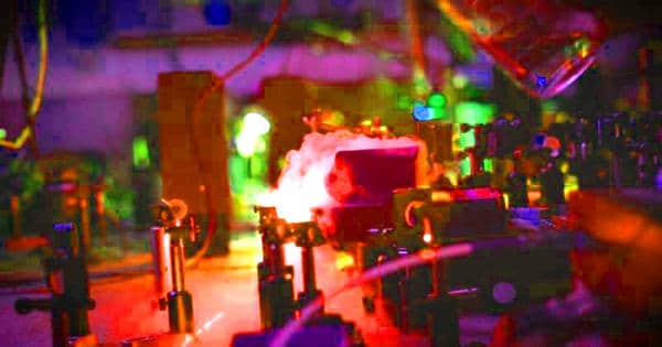
The Sussex team overcame these constraints by creating terahertz sources out of extremely thin materials (about 25 atomic layers). They were able to elicit the emission of short bursts of Terahertz radiation by illuminating an electronic-grade semiconductor with two different types of laser light, each oscillating at a different frequency or color.
Since the first demonstration of terahertz sources based on two-color lasers in the early 2000s, scientists in the field have been eagerly awaiting this scientific breakthrough. Two-color terahertz sources based on special gas mixtures such as nitrogen, argon, or krypton are among the best performing sources on the market today. Semiconductors, which are widely used in electronic technologies, have largely remained out of reach for this type of terahertz generation mechanism.