Superconducting contacts have been added to an ultrathin semiconductor by researchers. These ultrathin materials with novel electronic and optical properties have the potential to enable previously unimagined applications. They are expected to give rise to new quantum phenomena and find use in quantum technology when combined with superconductors.
For the first time, researchers at the University of Basel have outfitted an ultrathin semiconductor with superconducting contacts. These ultrathin materials with novel electronic and optical properties have the potential to enable previously unimagined applications. They are expected to give rise to new quantum phenomena and find use in quantum technology when combined with superconductors.
Semiconductors play a critical role in electronics, and thus in our daily lives, whether in smartphones, televisions, or building technology. In contrast to metals, electrical conductivity can be adjusted by applying a voltage and thus switching the current flow on and off.
Researchers are focusing on the development of new components made up of a single layer (monolayer) of semiconducting material in order to find future applications in electronics and quantum technology. Some naturally occurring semiconducting materials contain monolayers of this type, which are stacked to form a three-dimensional crystal. Researchers can separate these layers, which are no thicker than a single molecule, in the lab and use them to construct electronic components.
Researchers have equipped an ultrathin semiconductor with superconducting contacts. These extremely thin materials with novel electronic and optical properties could pave the way for previously unimagined applications.
New properties and phenomena
These ultrathin semiconductors promise to deliver unique characteristics that would otherwise be difficult to control, such as the use of electric fields to influence electron magnetic moments. Furthermore, complex quantum mechanical phenomena occur in these semiconducting monolayers, which could have applications in quantum technology.
Scientists from all over the world are looking into how these thin semiconductors can be stacked to create new synthetic materials known as van der Waals heterostructures. However, they have yet to combine such a monolayer with superconducting contacts in order to delve deeper into the properties and peculiarities of the new materials.
Superconducting contacts
A team of physicists led by Dr. Andreas Baumgartner from Professor Christian Schönenberger’s research group at the Swiss Nanoscience Institute and the Department of Physics at the University of Basel has for the first time fitted a monolayer of the semiconductor molybdenum disulfide with superconducting contacts.
This combination of semiconductor and superconductor is so intriguing because experts anticipate that components of this type will exhibit novel properties and physical phenomena.
“In a superconductor, electrons arrange themselves into pairs, like partners in a dance – with strange and wonderful consequences, such as the flow of electrical current without resistance,” explains Baumgartner, the study’s project manager. “In the semiconductor molybdenum disulfide, on the other hand, electrons dance in a strange solo routine that also incorporates their magnetic moments. Now we want to see which new and exotic dances the electrons agree on when we combine these materials.”
Suitable for use as a platform
Electrical measurements at the low temperatures required for superconductivity – just above absolute zero (-273.15°C) – clearly show the effects caused by the superconductor; for example, single electrons are no longer allowed at certain energies. In addition, the researchers discovered evidence of strong coupling between the semiconductor layer and the superconductor.
“Strong coupling is a key component in the new and exciting physical phenomena that we expect to see in such van der Waals heterostructures but have never been able to demonstrate,” says Mehdi Ramezani, the study’s lead author.
“Of course, we’re always hoping for new applications in electronics and quantum technology,” Baumgartner says. “The vertical contacts we developed for the semiconductor layers can, in theory, be applied to a wide range of semiconductors. Our measurements show that these hybrid monolayer semiconductor components are indeed possible, possibly even with other, more exotic contact materials, paving the way for future research “He continues.
Elaborate fabrication process
The creation of the new component in a sandwich made of various materials necessitates a large number of different steps. Contaminations must be avoided at all stages because they seriously impair the transport of electrical charges.
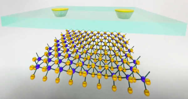
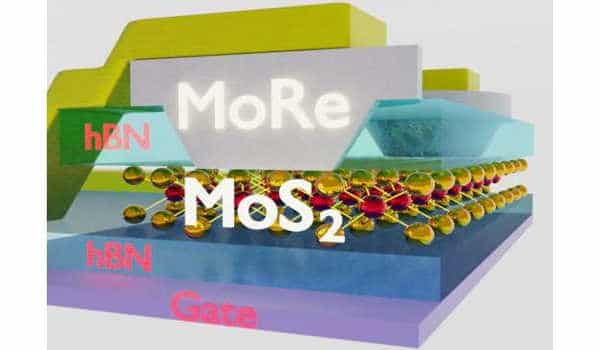
To shield the semiconductor, the researchers sandwich a monolayer of molybdenum disulfide between two thin layers of boron nitride, through which the contacts were previously etched vertically using electron-beam lithography and ion etching. They then apply a thin layer of molybdenum rhenium as a contact material, which retains its superconducting properties even in the presence of strong magnetic fields.
In a glove box, the researchers stack the boron nitride layer onto the molybdenum disulfide layer and combine the underside with another layer of boron nitride as well as a layer of graphene for electrical control. The elaborate van der Waals heterostructure is then placed on top of a silicon/silicon-dioxide wafer by the researchers.