
For decades, silicon-based semiconductors enabled field-effect transistors, which fueled the electronics revolution. However, in recent years, manufacturers have encountered hard physical limits to further silicon chip size reductions and efficiency gains. As a result, scientists and engineers are searching for alternatives to traditional metal-oxide semiconductor (CMOS) transistors.
“Organic semiconductors offer several distinct advantages over conventional silicon-based semiconducting devices: they are made from abundantly available elements such as carbon, hydrogen, and nitrogen; they offer mechanical flexibility and low manufacturing costs; and they can be easily fabricated at scale,” says UC Santa Barbara engineering professor Yon Visell, who is part of a group of researchers working with the new materials.
“Perhaps more importantly, the polymers themselves can be crafted using a wide variety of chemistry methods to endow the resulting semiconducting devices with interesting optical and electrical properties. These properties can be designed, tuned or selected in many more ways than can inorganic (e.g., silicon-based) transistors.”
The design flexibility that Visell describes is exemplified in the reconfigurability of the devices reported by UCSB researchers and others in the journal Advanced Materials.
Reconfigurable logic circuits are particularly appealing as post-CMOS electronics candidates because they simplify circuit design while increasing energy efficiency. Organic electrochemical transistors (OECTs), a recently developed class of carbon-based (as opposed to silicon- or gallium-nitride-based) transistors, have been shown to be well-suited for reconfigurable electronics.
In a recent paper, chemistry professor Thuc-Quyen Nguyen, who directs the UCSB Center for Polymers and Organic Solids, and co-authors including Visell describe a breakthrough material – a soft, semiconducting carbon-based polymer – that has distinct advantages over the inorganic semiconductors currently used in conventional silicon transistors.
Organic semiconductors offer several distinct advantages over conventional silicon-based semiconducting devices: they are made from abundantly available elements such as carbon, hydrogen, and nitrogen; they offer mechanical flexibility and low manufacturing costs; and they can be easily fabricated at scale.
Professor Yon Visell
Conjugating for Conductivity
CPE-K, or conjugated polyelectrolyte, is made up of a central conjugated backbone with alternating single and double bonds and multiple charged side chains with ions attached. “Having conjugated bonds throughout the polymer makes it conductive because the delocalized electrons have high mobility across the length of the polymer,” says lead author Tung Nguyen-Dang, a postdoctoral researcher in Nguyen’s lab and Visell’s co-adviser. “In this molecular design, you’re combining two classic materials: polymer and semiconductor.”
The material was created using artificial intelligence (AI). “You can make a material through trial and error,” Nguyen says. “You can make a bunch of them and hope for the best, and maybe one out of twenty works or has interesting properties; however, we worked with a professor at California State Northridge, Gang Lu, who used AI to select building blocks and do calculations to get a rough idea of how to proceed, given the energy level and properties we were aiming for.”
Figuring out Reconfigurability
One significant advantage of CPE-K is that it enables reconfigurable (“dual-mode”) logic gates, which can be switched on the fly to operate in either depletion mode or accumulation mode by adjusting the gate voltage. Before applying any gate voltage in depletion mode, the current flowing through the active material between the drain and the source is initially high (a.k.a. the ON state). When the gate voltage is applied, the current decreases and the transistor turns off. Accumulation mode is the inverse: without a gate voltage, the transistor is in an OFF state, and applying a gate voltage produces more current, causing the device to switch to an ON state.
“Conventional electronic logic gates, which are the building blocks for all digital circuits found in computers or smart phones, are hardware that do only one job,” Nguyen says. “For example, an AND gate has two inputs and one output; if all of the inputs are 1, the output will be 1. Similarly, a NOR gate has two inputs and one output, but if all of its inputs are 1, the output will be 0. Electronic gates are made up of transistors, and changing their configuration (for example, from an AND gate to a NOR gate) necessitates invasive modification, such as dismantling, which is usually too complicated to be practical.
“Reconfigurable gates, like the one we show, can behave as both types of logic gates, switching from AND to NOR and vice versa by changing only the gate voltage,” she continues. “Currently in electronics, functionality is defined by structure, but in our device you can change the behavior and make it something else just by changing the voltage applied to it. If we scale up this invention from a single gate to much more complex circuits consisting of many such reconfigurable gates, we can envision a powerful piece of hardware that can be programmed with many more functionalities than conventional ones having the same number of transistors.”
Another benefit of CPE-K-based OECTs is that they can operate at extremely low voltages, making them suitable for use in personal electronics. This, combined with the material’s flexibility and biocompatibility, makes it a promising candidate for implanted biosensors, wearable devices, and neuromorphic computing systems in which OECTs could serve as artificial synapses or non-volatile memories.
“Our colleague at the University of Cambridge in England is developing devices that can monitor the drop in glucose levels in the brain that occurs just before a seizure,” Nguyen says of a collaborator. “And, once detected, another device — a microfluidic device — will deliver a drug locally to prevent the process from occurring.”
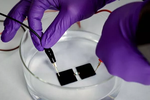
According to Nguyen, devices made of CPE-K feature concurrent doping and de-doping depending on the type of ions. “You build the device and immerse it in a liquid electrolyte, which is sodium chloride [table salt] dissolved in water,” she explains. “Applying a positive voltage to the gate will then cause the sodium to migrate into the CPE-K active layer. Alternately, you can reverse the polarity of the gate voltage and drive chloride to the active layer. Each scenario generates a different type of ion injection, and it is those ions that allow us to change the modes of device operation.”
Self-doping also streamlines the manufacturing process by eliminating the step of adding dopants. “When you add a dopant, it is not always evenly distributed throughout the volume of the material,” Nguyen explains. “Organic doping materials tend to cluster together rather than disperse. However, because our material does not require that step, you do not encounter the problem of uneven dopant distribution. You also avoid the entire process of optimizing the dopant and determining the proper mix and proportions, which all add steps and complicate the process.”