Construction of Junction Transistor (p-n-p and n-p-n)
A transistor is a three-terminal semiconducting device whose output current, potential difference, and power are controlled by input current. By connecting two semiconducting diodes side by side a semiconducting triode or transistor is formed. 1. Bardeen and W. H. Brighton in 1948 first invented transistor in America. After its invention, this transistor has created a revolution in the electronic world. An integral component of electronic instruments is the transistor.
Construction
From a pure semiconductor, a transistor is produced at high temperature and by using a controlled technique. Normally two types of transistors are produced, viz— point contact transistor and junction transistor.
![]()
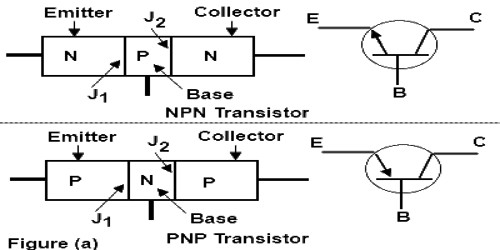
But nowadays most of the transistors used are junction transistors. Transistors are of two types, viz. (a) n-p-n transistor, and (b) p-n-p transistor. A transistor has three elements, viz— emitter (E), base (B), and collector (C). In figure (a) and (b) block diagrams of n-p-n and p-n-p transistors and their symbols have been shown.
If between two n-type semiconducting crystals a p-type semiconducting crystal is connected side by side in a special technique, then, n-p-n transistor is formed. Again if between two p-type crystals and n-type crystal is connected, then the p-n-p transistor is formed. This joining is not like gluing or not of soldering. In a semiconducting crystal p or n-type impurities are mixed in a controlled way and successively n or p-type impurities are mixed at high temperature on it and finally, p or n-type impurities are mixed on it and thus n-p-n or p-n-p transistor is formed. The middle portion called base is made very thin and a small amount of impurities is added in this section, so that charge carriers from the emitter can cross easily by travelling small distance and do not mix with opposite charges to be neutralized. The emitter part is quite thick and heavily doped. The collector part is the thickest of all so that heat generated in it can easily be radiated. Besides collector is also heavily doped. There are two junctions in a transistor, viz – emitter-base junction and base-collector junction. It has been mentioned earlier that by the combination of two p-n junctions a transistor is made. One junction is made forward biased and the other one is made reverse biased. A resistance of the forward biased junction is very small compared to the reverse biased junction. Weak signal is applied to the low resistance junction and output is taken from the high resistance junction.
In the figure, biasing of n-p-n and p-n-p transistors has been shown. So, it is seen that a transistor transfers a signal from lower resistance to higher resistance. It transfers current through resistance; hence nomenclature has been made transfer resistor, in that transistor. In other words, it can be said that in a small semiconductor output current, voltage and power are controlled by the input current, hence it is called a transistor.