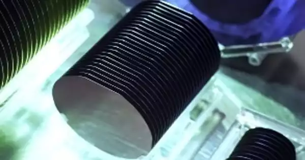
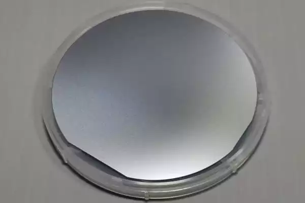
Gallium antimonide (GaSb) is a semiconducting III-V family gallium and antimony combination. Its lattice constant is around 0.61 nm. The band gap is 0.67 eV. GaSb is the highest refractive index semiconducting substrate. It is a highly conductive material that can be used to create heat photovoltaic cells and detectors.
GaSb is an antimony and gallium semiconductor that belongs to the III to V semiconductor family. GaSb has a lattice constant of 0.61 nm. GaSb’s unusual lattice structure allows it to be used in complex semiconductor applications. For example, in January 2013, researchers at Northwestern University’s Centre for Quantum Devices created the first dual-mode passive and active infrared camera device constructed of gallium antimonide/indium arsenide.
Solar cells made of GaSb have shown to be the most efficient semiconductors. The most significant disadvantage is the cost. The high prices of GaSb make wafers unprofitable when compared to silicon-based solar cells. However, researchers should not be afraid to investigate these solar cells. A homeowner’s roof may one day be regarded a solar commodity, and higher-efficiency cells may make a smaller roof as viable as a larger roof with silicon solar panels.
Properties
The band gap of gallium antimonide (GaSb) has the same lattice constants as other wafers in the III-V wafer group. Because of this characteristic, GaSb is an ideal substrate for solar cells. GaSb’s energy density and efficiency make the substrate a superb, but costly, choice for solar cell applications. In addition, gasb wafers are utilized in infrared detectors and lasers. Tellerium-doped GaSb wafers can be used to manufacture ethermal photovoltaic and microwave devices.
- Molecular Weight: 191.48
- Appearance: Crystalline solid
- Melting Point: 710 °C
- Boiling Point: N/A
- Density: 5.62 g/cm3
- Solubility in H2O: N/A
- Exact Mass: 189.829399
Electrical Properties
- Mobility and Hall Effect
- Transport Properties in High Electric Field
- Impact Ionization
- Recombination Parameters
History
Victor Goldschmidt created the intermetallic compound GaSb in 1926 by directly combining the elements in an inert gas atmosphere and reporting on GaSb’s lattice constant, which has subsequently been updated. Gallium phosphide and gallium arsenide were also produced by Goldschmidt. Koster and Greenfield studied the Ga-Sb phase equilibria in 1955.
Applications
Infrared detectors, infrared LEDs and lasers, transistors, and thermophotovoltaic systems can all benefit from GaSb. This material is extremely versatile and can be used in a variety of applications. It can be found in infrared LEDs, thermo-photovoltaic systems, photoresistors, and a variety of other devices. Because it is light and durable, it is an excellent choice for many semiconductors. It is also capable of withstanding high voltage. Gallium antimonide is a highly sought-after substance due to these properties. And as a result, it is an ideal material for a variety of uses. It finds applications in:
- Infrared detectors,
- Infrared LEDs,
- Transistors,
- Lasers,
- Thermophotovoltaic systems.