New Innovation Advances Optical Light Microscopy
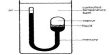
The new and conventional optical microscope methods are labeled (EC) and (No EC), respectively. Microscopy has come a long way since the compound microscopes of the 17th century that Hooke used, where two convex lenses produced a magnified image. New Illinois ECE research is advancing the field of optical microscopy, giving the field a critical new tool to solve challenging problems across many fields of science and engineering including semiconductor wafer inspection, nanoparticle sensing, material characterization, biosensing, virus counting, and microfluidic monitoring. As well as optical microscopy, which uses primarily visible light, we now have a host of other imaging techniques based on electrons, X-rays, atomic forces, and other approaches besides.
“Their work, published in Nature Communications opens new doors to using optical microscopy to unravel difficult problems that impact our daily lives.”
The question is often asked, “Why can we not see or sense nanoscale objects under a light microscope?” Many of these achieve far greater resolutions than optical microscopy, so can this traditional technique ever catch up? What will then limit its scope, and why even bother trying to improve something so old-fashioned?
Since its discovery in 17th-century, optical microscopy has been acting as an indispensable tool in the exploration of the unknown microworld, especially in biomedical fields. However, the Illinois ECE research team, led by Illinois ECE Professor Lynford L Goddard, along with postdoc Jinlong Zhu, and Ph.D. student Aditi Udupa, is challenging these cornerstone principles with a brand-new optical framework.
Their work, published in Nature Communications opens new doors to using optical microscopy to unravel difficult problems that impact our daily lives. “Our work is significant not only because it advances scientific understanding of optical imaging but also because it enables researchers to directly visualize unlabeled objects that have deep sub-wavelength separations. We can see the nanoscale structure without performing any image post-processing” said Goddard.
The team’s breakthroughs began in May 2018 when Zhu and Goddard stumbled upon a remarkable result in one of their simulations. “At the time, we were conducting a theoretical study on wafer defect inspection and needed to build a simulation tool to model how light propagates through a microscope system. When we saw the simulation result for one of the configurations, we were quite confused by it,” Goddard recalls. “We worked day and night for the next three months trying to understand the physics behind it. Once we developed a closed-form analytic expression that explained what was going on, we could devise an experiment to test our hypotheses.”
However, it would take another five months of trial and error to learn how to build and align the optical system such that the experimental configuration replicated the model assumptions. Meanwhile, Ms. Udupa fabricated suitable test samples at both the Holonyak Micro and Nanotechnology Laboratory and the Materials Research Laboratory with the assistance of Dr. Edmond Chow and Dr. Tao Shang. In January 2019, the team finally realized the necessary experimental conditions and directly visualized their first set of deep sub-wavelength objects.
“Using a standard optical microscope to visualize nanometric objects is extremely challenging not only because of the diffraction barrier but also the weak signal,” said Zhu. “Our experiment had to utilize two new and interesting physical concepts, anti-symmetric excitation and non-resonance amplification, to boost the signal-to-noise ratio of the nanoscale objects.”
The team demonstrated the technique can sense both free-form and fixed-form nanoscale objects across a wide field of view (726-μm × 582-μm) using a low numerical aperture objective (0.4 NA). Zhu explains, “We were quite lucky that some of the nanowires on our test sample shown above had fabrication imperfections. This allowed us to demonstrate the visualization of sub-20 nm defects in a semiconductor chip. In the future, one may also apply our method for the visualizable sensing of biological objects (e.g., viruses or molecule clusters) by choosing nanowires with optimized geometry and proper refractive index and patterning functional groups around nanowires. Once target analytes are trapped, they act as objects that may be directly visualized from the optical images.”