The concept about Electron and Hole
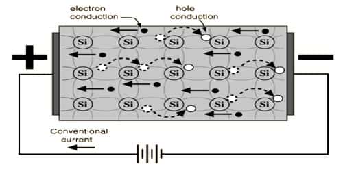
At room temperature electron and hole are produced in the pair in an intrinsic semiconductor. When an electric field is applied then electric current flow is performed in two ways. For example, by electrons land by holes. When the temperature is increased then due to thermal energy some valence electrons enter into the conduction band and become free electrons. Holes and electrons are the two types of charge carriers responsible for current in semiconductor materials. Now whenever an electron enters into the conduction band, then a vacant space or a hole is produced in the valence band. Due to the influence of potential difference or electric field flow of both electrons and holes are produced. The electron is a negative charge carrier whereas the hole is a positive charge carrier.
Most familiar intrinsic semiconductors are germanium and silicon. The energy gap between their valence band and conduction band are 0.72 eV and 1.l eV respectively. At room temperature, some electrons from the valence band can cross this small energy gap and is accumulated in the conduction band. As a result, an equal number of holes and electrons are produced [Figure]. This phenomenon is called electron-hole pair Production.
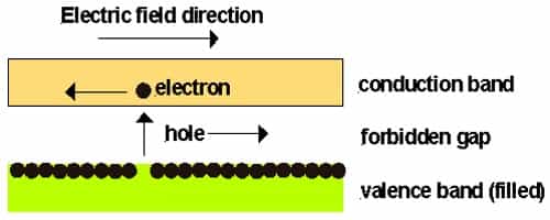
Alternately it can be said that due to the transfer of electrons in the conduction band positively charged holes are produced in the valence band. At the temperature above absolute zero, if the electric field is applied then conduction electrons move towards anode and holes move towards the cathode. So, it can be said that the current flow in the semiconductor is the flow of electrons and holes in the valence and conduction bands in opposite directions.