Advanced nanofabrication techniques such as electron beam lithography, focused ion beam milling, and even self-assembly approaches are frequently used to create precise arrays of nanoLEDs. As these techniques are refined, they will be able to produce more accurate and densely packed arrays. Researchers can now ‘grow’ halide perovskite nanocrystals with precise control over the location and size of each individual crystal before integrating them into nanoscale light-emitting diodes using a new platform.
Halide perovskites are a class of materials that have piqued the interest of researchers due to their superior optoelectronic properties and potential applications in devices such as high-performance solar cells, light-emitting diodes, and lasers.
These materials are mostly used in thin-film or micron-sized device applications. Precisely integrating these materials at the nanoscale could pave the way for even more amazing applications, such as on-chip light sources, photodetectors, and memristors. However, because this delicate material can be damaged by traditional fabrication and patterning techniques, achieving this integration has remained difficult.
To overcome this barrier, MIT researchers developed a technique that allows individual halide perovskite nanocrystals to be grown on-site with precise control over location to within 50 nanometers. (The thickness of a sheet of paper is 100,000 nanometers.) This technique can also precisely control the size of the nanocrystals, which is important because size affects their properties. Since the material is grown locally with the desired features, conventional lithographic patterning steps that could introduce damage are not needed.
As our work shows, it is critical to develop new engineering frameworks for integration of nanomaterials into functional nanodevices. By moving past the traditional boundaries of nanofabrication, materials engineering, and device design, these techniques can allow us to manipulate matter at the extreme nanoscale dimensions, helping us realize unconventional device platforms important to addressing emerging technological needs.
Farnaz Niroui
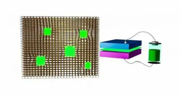
The technique is also scalable, versatile, and compatible with conventional fabrication steps, allowing for the incorporation of nanocrystals into functional nanoscale devices. The researchers used this to make arrays of nanoscale light-emitting diodes (nanoLEDs), which are tiny crystals that emit light when activated electrically. Optical communication and computing, lensless microscopes, new types of quantum light sources, and high-density, high-resolution displays for augmented and virtual reality could all benefit from such arrays.
“As our work shows, it is critical to develop new engineering frameworks for integration of nanomaterials into functional nanodevices. By moving past the traditional boundaries of nanofabrication, materials engineering, and device design, these techniques can allow us to manipulate matter at the extreme nanoscale dimensions, helping us realize unconventional device platforms important to addressing emerging technological needs,” says Farnaz Niroui, the EE Landsman Career Development Assistant Professor of Electrical Engineering and Computer Science (EECS), a member of the Research Laboratory of Electronics (RLE), and senior author of a new paper describing the work.
Tiny crystals, huge challenges
Using traditional nanoscale fabrication techniques, integrating halide perovskites into on-chip nanoscale devices is extremely difficult. A thin film of fragile perovskites could be patterned using lithographic processes, which require solvents that could damage the material. Another method involves forming smaller crystals in solution and then picking and placing them in the desired pattern.
“In both cases, there is a lack of control, resolution, and integration capability, which limits how the material can be extended to nanodevices,” says Niroui. Instead, she and her team devised a method to “grow” halide perovskite crystals in precise locations directly onto the desired surface, where the nanodevice will then be fabricated.
The solution used in nanocrystal growth is localized, which is central to their process. To accomplish this, they design a nanoscale template with small wells that contain the chemical process by which crystals grow. They alter the surface of the template and the interior of the wells to control a property known as “wettability,” ensuring that a solution containing perovskite material does not pool on the template surface and is confined inside the wells.
“Now, you have these very small and deterministic reactors within which the material can grow,” she says. That is exactly what occurs. They apply a solution containing halide perovskite growth material to the template, and the material grows and forms a tiny crystal in each well as the solvent evaporates.
A versatile and tunable technique
The researchers discovered that the shape of the wells is crucial in controlling the positioning of the nanocrystals. Due to the influence of nanoscale forces, crystals have an equal chance of being placed in each of the well’s four corners when square wells are used. That may be sufficient for some applications, but for others, greater precision in nanocrystal placement is required.
By changing the shape of the well, the researchers were able to engineer these nanoscale forces in such a way that a crystal is preferentially placed in the desired location. As the solvent evaporates inside the well, the nanocrystal experiences a pressure gradient that creates a directional force, with the exact direction being determined using the well’s asymmetric shape.
“This allows us to have very high precision, not only in growth, but also in the placement of these nanocrystals,” Niroui says. They also found they could control the size of the crystal that forms inside a well. Changing the size of the wells to allow more or less growth solution inside generates larger or smaller crystals.
They demonstrated the technique’s effectiveness by creating precise arrays of nanoLEDs. In this method, each nanocrystal is converted into a nanopixel that emits light. These high-density nanoLED arrays have the potential to be used in on-chip optical communication and computing, quantum light sources, microscopy, and high-resolution displays for augmented and virtual reality applications.
The researchers hope to investigate more potential applications for these tiny light sources in the future. They also want to test the limits of how small these devices can be and work on incorporating them effectively into quantum systems. Aside from nanoscale light sources, the process opens up new avenues for developing halide perovskite-based on-chip nanodevices.