Organic semiconductors have a reputation for being energy-efficient materials in organic light-emitting diodes (OLEDs), which are used in large-area displays. The energy gap between electronic states is a critical parameter in these and other applications, such as solar cells.
Tuning the energy gap by blending different semiconducting molecules to optimize device performance remains a challenge for organic semiconductors, as it has been for inorganic semiconductors. Scientists have now demonstrated how to achieve this goal.
Organic semiconductors have a reputation for being energy efficient materials in organic light emitting diodes (OLEDs), which are used in large area displays. The energy gap between electronic states is a critical parameter in these and other applications, such as solar cells. It is responsible for determining the wavelength of light that is emitted or absorbed. It is preferable if this energy gap can be adjusted on a continuous basis. In fact, an appropriate method for inorganic materials already exists: blending.
It is based on engineering the band gap in a material by substituting atoms. This enables continuous tunability, as seen in aluminum gallium arsenide semiconductors. Unfortunately, because of their different physical properties and molecule-based construction paradigm, this is not transferable to organic semiconductors, making continuous band gap tuning much more difficult.
Tuning the energy gap by blending different semiconducting molecules to optimize device performance. Now, scientists demonstrated how to reach this goal.
However, in their most recent publication, scientists at the Center for Advancing Electronics Dresden (cfaed, TU Dresden) and the Cluster of Excellence “e-conversion” at TU Munich, in collaboration with partners from the University of Würzburg, HU Berlin, and Ulm University, for the first time realized energy-gap engineering for organic semiconductors through blending.
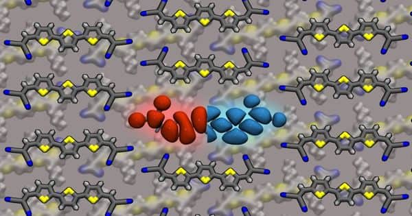
Atomic substitutions can shift the energy levels closer together in inorganic semiconductors, reducing the band gap (“band-gap engineering”). Band structure modifications by blending organic materials, on the other hand, can only shift the energy levels concertedly up or down. This is because of the strong Coulomb effects that can be used in organic materials, but it has no effect on the gap. “It would be very interesting to change the gap of organic materials by blending, to avoid the lengthy synthesis of new molecules,” says TU Dresden Prof. Karl Leo.
Tuning the energy gap by combining different semiconducting molecules to optimize device performance is a well-established procedure for inorganic semiconductors, but it remains a challenge for organic semiconductors. Scientists from TU Dresden have now demonstrated how to achieve this goal in collaboration with researchers from TU Munich, the University of Würzburg, HU Berlin, and Ulm University.
The researchers devised a novel method by combining the material with mixtures of similar molecules of varying sizes. “The key discovery is that all molecules arrange in specific patterns that are allowed by their molecular shape and size,” says Frank Ortmann, a TU Munich professor and group leader at the Center for Advancing Electronics Dresden (cfaed, TU Dresden). “This causes the desired change in the dielectric constant and gap energy of the material.”
By simulating the structures of the blended films as well as their electronic and dielectric properties, Frank Ortmann’s group was able to clarify the mechanism. X-ray scattering measurements performed by Prof. Stefan Mannsfeld’s Organic Devices Group at cfaed confirmed a corresponding change in molecular packing depending on the shape of the blended molecules. Katrin Ortstein and her colleagues at Prof. Karl Leo’s group at TU Dresden performed the majority of the experimental and device work.
The findings of this study were recently published in the journal Nature Materials. While this demonstrates the feasibility of this type of energy-level engineering strategy, its application in optoelectronic devices will be investigated in the future.