Scientists have used two powerful, cutting-edge techniques to investigate the physics of an unusual phase transition that converts a metal to an insulator. They investigated rare-earth nickelates, which are of great interest for developing new approaches in electronics.
“Phase transitions” are an important phenomenon in the physical sciences. Despite their technical sounding names, they are phenomena that we all encounter on a daily basis: ice melting into liquid water or hot water evaporating as steam. Solid, liquid, and gas are three well-known “phases,” and when one transforms into another, this is referred to as a phase transition.
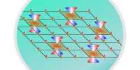
Rare-earth nickelate oxides, also known as nickelates, have piqued the interest of researchers because they exhibit an electronic phase transition that could be used in future electronic devices. As temperature decreases, this phase transition involves changing from a metallic state that conducts electricity to an electrically insulating state.
Behind this behaviour is a strong interaction between the electronic properties of these compounds and their “lattice” structure — the well-ordered arrangement of atoms that forms a crystal. However, understanding the true nature of this metal to insulator phase transition in nickelates and controlling it for potential electronic devices necessitates understanding how each characteristic phase emerges and evolves across the transition.
Scientists at EPFL and the University of Geneva have combined two powerful, cutting-edge techniques to uncover the physics behind an exotic phase transition that turns a metal into an insulator.
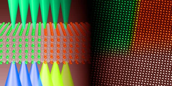
EPFL and University of Geneva researchers have now combined two cutting-edge techniques to achieve nanoscale mapping of each distinct electronic phase. The study was led by Dr Duncan Alexander at EPFL’s School of Basic Sciences and Professor Jean-Marc Triscone’s group at the University of Geneva, and it was published in the journal Nano Letters.
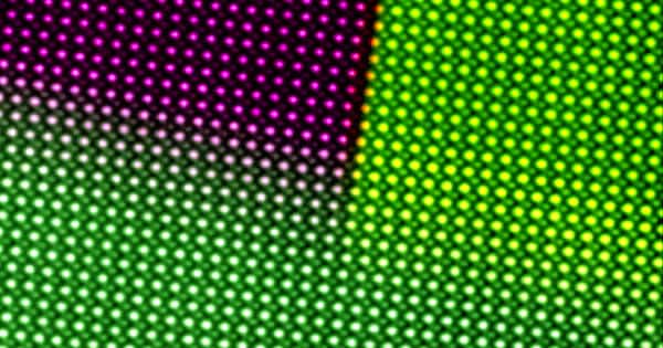
Dr. Bernat Mundet, the study’s first author, says: “New atomic-scale characterization techniques are required to fully understand the physics of novel electronic materials and control them in devices. In this regard, we were able to precisely determine the metallic and insulating regions of atomically engineered devices made from two nickelate compounds with near atomic resolution for the first time. We believe that our methodology will contribute to a better understanding of the physics of this important class of electronic materials.”
The researchers used scanning transmission electron microscopy (STEM) with aberration correction and monochromated electron energy-loss spectroscopy (EELS). STEM images are created by scanning a beam of electrons focused to a spot about 1 ngstrom in size across a sufficiently thin specimen, in this case a sliver of nickelate, and collecting the transmitted and scattered electrons with annular detectors. Despite its technical difficulties, this technique allows researchers to precisely visualize a crystal’s lattice structure, atomic row by atomic row.
Electrons passing through the annular detector’s central hole are instead collected for the second technique, EELS. Some of these electrons have previously lost energy as a result of their interactions with the nickelate crystal’s Ni atoms. We can determine whether the nickelate compound is metallic or insulating by measuring how this energy difference changes.
Because all electrons are scattered and collected at the same time, the researchers were able to correlate the electronic state changes in the different nickelate compounds with the associated lattice positions. This method enabled them to map the spatial configuration of their metallic or insulating regions for the first time, with a very high spatial resolution of around 3.5 ngstroms (0.35 nanometers). The method will be useful for studying and guiding the atomic engineering of these novel electronic materials.
“The latest electron microscopes provide us with an incredible ability to measure a variety of materials’ physical properties with atomic or nanometric spatial resolution,” says Duncan Alexander. “We take an exciting step forward in this domain by proving that we can measure the changes in electronic state across a thin film structure precisely made from two different nickelates by pushing the capabilities of EPFL’s Titan Themis microscope to their limits. Our method opens up new avenues for studying the physics of these nickelate compounds, which have piqued the interest of researchers all over the world.”
“The combination of amazing artificial materials that exhibit a metal to insulator transition and very advanced electron microscopy has allowed for unprecedented detailed investigations of their electronic properties,” Jean-Marc Triscone adds. “In particular, it revealed whether the material is conducting or insulating at the atomic scale – an important question for better understanding these materials that may be used in future computing approaches.”