In order to realize the potential of semiconducting 2D materials, a necessary component for developing new atom-thick transistors that can overturn Moore’s Law, researchers had to overcome three excruciatingly challenging technological problems. It now seems possible to produce high-quality 2D materials on a commercial scale thanks to the efforts of a multi-institution research team.
Natural limitations imposed by the methods and materials employed in transistor fabrication pose a danger to the development of semiconductors. This obstacle to Moore’s Law has been lurking in the distance for some time, and forward-thinking researchers have been looking into and creating workarounds to provide the desired continual progress.
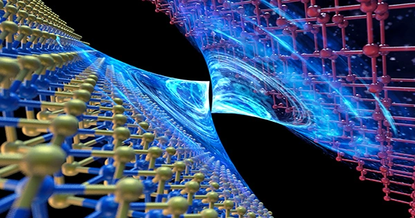
Replace silicon with so-called 2D materials to create 2D transistors is one of the semiconductor industry’s most viable strategies to gain momentum. Scientists studying 2D materials closely have identified a number of appealing characteristics that should contribute to delivering considerable gains to performance, efficiency, and scalability. For instance, the Components Research (CR) Group at Intel recently published nine papers, some of which advocated the use of novel 2D materials as a means of producing CPUs with more than a trillion transistors by the year 2030.
According to the multinational team of experts, three major obstacles to the commercialization of 2D materials have now been overcome, enabling the production of 2D materials in a single-crystalline form on silicon wafers. These difficulties were detailed particularly as follows:
Layer-by-layer 2D material growth under fine kinetic control, with a single domain, maintained for uniform thickness and wafer-scale controllability of layer numbers and crystallinity.
For more information on each of these issues and how the multi-institutional team’s approaches have been used to address them, read the complete paper. The research was described in a paper(opens in new tab) written by Nature magazine and titled “Non-epitaxial single-crystal 2D material development by geometric confinement.”
Sang-Hoon Bae, one of the project’s coordinators and a professor of mechanical engineering and materials science at Washington University in St. Louis’ McKelvey School of Engineering, appears to be confident in the significance of the study’s findings. We think that by enabling the creation of single domain layer-by-layer heterojunctions at the wafer scale, our constrained growth technique can enable the commercialization of all the remarkable achievements in the physics of 2D materials. “Our success will build a solid foundation for the integration of 2D materials into industrial settings.”
It can take years before 2D materials are used in real-world applications, as is the case with any research of this kind. That future, however, might be closer than you think thanks to businesses like Intel and Samsung being actively involved in this initiative and the fact that Intel already has 2D Gate All Around (GAA) transistors in its development pipeline.