Diamond is said to be the hardest of all elements in existence. However, out of many assumptions, diamonds still have excellent potential as a superior electronic material. Diamond is the hardest substance in the world. But it still has tremendous promise as an outstanding electronic material out of many standards. For the first time, a joint research team led by the City University of Hong Kong (CityU) has demonstrated a broad, uniform tensile elastic straining of micro-manufactured diamond arrays via a nano-mechanical approach. Their findings have shown the potential of strained diamonds as prime candidates for advanced functional devices in microelectronics, photonics, and quantum information technologies.
Researchers at the City University of Hong Kong (CityU) have demonstrated large, uniform tensile elastic straining of micro-fabricated diamond arrays through the nano-mechanical approach. Findings show the potential of strained diamonds as prime candidates for advanced functional devices in microelectronics, photonics, and quantum information tech.
For the first time, a collaborative research group has used a nano-mechanical technique to detect large and even tensile elastic straining of micro-fabricated diamond arrays. The team was led by Hong Kong City University (CityU). The project was co-led by Dr. Lu Yang, Associate Professor at the Department of Mechanical Engineering (MNE) at CityU, and by researchers at the Massachusetts Institute of Technology (MIT) and the Harbin Institute of Technology (HIT). Their results have recently been published in the research journal Science, entitled “Achieving large uniform tensile elasticity in a micro-fabricated diamond.”
Research findings have shown that stretched diamonds may serve as key candidates for next-generation practical devices used in photonics, microelectronics and quantum information technologies. “This is the first time showing the extremely large, uniform elasticity of diamond by tensile experiments. Our findings demonstrate the possibility of developing electronic devices through ‘deep elastic strain engineering’ of micro-fabricated diamond structures,” Dr. Lu said.

Diamond: “Mount Everest” of electronic materials
Well known for their hardness, the commercial uses of diamonds are generally cutting, digging, or grinding. Diamond is often known to be a high-performance electronic and photonic material due to its ultra-high thermal conductivity, excellent electric charge carrier mobility, high breakdown power, and ultra-wide bandgap. Bandgap is a semiconductor’s main property, and a large bandgap facilitates the operation of high-power or high-frequency applications. “That’s why diamond can be considered as ‘Mount Everest’ of electronic materials, possessing all these excellent properties,” Dr. Lu said.
However, the wide belt gap and the close diamond crystal structure make it difficult to ‘dope,’ a typical method of modulating the electronic semiconductor properties during processing, thereby hindering the industrial use of diamonds in electronic and optoelectronic products. The potential solution is “strain engineering,” which includes the introduction of very large lattice strains, the alteration of the electronic band arrangement, and the related functional properties. However, owing to its exceptionally high hardness, it was deemed “impossible” for diamonds.
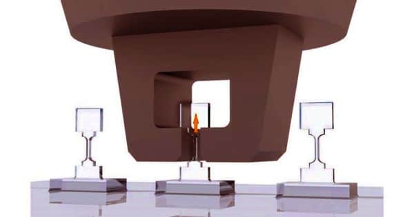
Uniform tensile straining across the sample
First, a team of micro-manufactured single-crystalline diamond samples from solid, single-crystal diamonds. The samples were in a bridge-like shape—about one micrometer long and 300 nanometers high, with both ends wider for grasping. The diamond bridges were then uniaxially extended inside the electron microscope in a well-controlled fashion. Under constant and controllable loading-unloading cycles of quantitative tensile tests, the diamond bridges exhibited a very uniform, broad elastic deformation of about 7.5 percent of the strain across the entire gage segment of the specimen, rather than deformation at the localized bending region. And they recovered their original shape after unloading.
By further refining the sample geometry using the American Society for Research and Materials (ASTM) norm, they reached an overall uniform tensile strain of up to 9.7%, which also exceeded the maximum local value in the 2018 analysis and was similar to the theoretical elastic limit of the diamond. More specifically, the team also realized the elastic straining of micro-manufactured diamond arrays to demonstrate the nature of the strained diamond system.
Tuning the bandgap by elastic strains
The team then carried out calculations of the Density Functional Theory (DFT) to quantify the effect of elastic straining on the electronic properties of the diamond from 0 to 12 percent. The simulation results revealed that the diamond bandgap usually decreased as the tensile strain increased, with the highest bandgap reduction from around 5 eV to 3 eV at about 9 percent of the strain in a particular crystalline orientation. The team conducted an electron energy-loss spectroscopy study on a pre-stressed diamond sample and confirmed this diminishing pattern.
Their measurement findings also revealed that, surprisingly, the bandgap could shift from indirect to direct, with tensile strains greater than 9 percent along with another crystalline orientation. Direct bandgap in semiconductors means that an electron will actually emit a photon, allowing for certain optoelectronic applications with higher performance.
These results are an early phase in the advancement of deep elastic strain engineering for micro-manufactured diamonds. By nano-mechanical approach, the team has shown that the composition of the diamond band can be modified and, most significantly, these modifications can be continuous and reversible, allowing diverse applications, from micro/nano-electromechanical systems (MEMS/NEMS), strain-engineered transistors to novel optoelectronic and quantum technologies. “I believe a new era for a diamond is ahead of us,” Dr. Lu said.
These findings are an early step in achieving deep elastic strain engineering of micro-fabricated diamonds.