Working Principle of p-n-p transistor
The term ‘P-N-P’ stands for positive, negative, positive and also known as sourcing. When a single n-type semiconductor layer is sandwiched between two p-type semiconductor layers, a p-n-p transistor is formed.
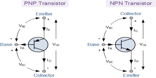
In fig. (a) and (b) biasing system has been shown for a “p-n-p transistor”. Holes from p region enter into the base region and as a collector is more negative so holes speedily move to the collector and a large current is produced. In this case, emitter-base junction is forward biased and the collector-base junction is reverse biased. Due to forward biasing holes of the emitter region move to the base region and create emitter current IE.
![]()
Again, holes entering into the n-region base intend to combine with the electrons there. As the base is very thin, so only about 5% holes combine with electrons in the base and create base current IB. Rest 95% holes move to the collector region and produce collector current IC. In this way, almost total emitter current flows in the collector circuit.
Due to the flow of charges in the emitter region, the generated current is called emitter current (IE), in the base region due to the combination of holes and current a base current (IB) is produced and due to the current of charges in the collector region the collector current (IC) is produced. Base current does not go to the collector current. This current comes out through the base terminal. So, it is seen that total emitter current does not flow to the collector region. i.e., the collector current is less than the emitter current. In this case, IE, IB, and IC are related in the following way:
IE = IB + IC