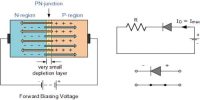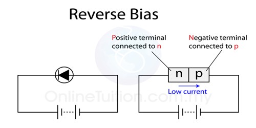
If a p-type and n-type semiconductors are connected by a special technique then the junction surface is called a p-n junction. It is one of the simplest semiconductor devices around, and which has the characteristic of passing current in only one direction only. The process by which, a p-n junction diode blocks the electric current in the presence of applied voltage is called reverse-biased p-n junction diode.
Characteristics of reverse biasing –
- Inside the junction diode, current flow is due to both the majority carriers; but in the external circuit, current flow is only clued to electrons.
- In reverse bias current of μA is available.
- No substantial change in current occurs up to a fixed amount of applied potential difference.
- A width of the depletion layer progressively increases with increasing reverse bias.
From the above discussion, it is realized that p-n junction is a unidirectional device which generates current flow in one direction. The p-type region of a diode is called the anode and the n-type region is called cathode. In the figure, a triangle indicates the direction of current in the forward bias.
Example: What happens in the depletion layer during reverse bias?
When the junction is in reverse bias then diffusion of charges stops. So the width of the depletion region increases. The main flow of the current of electrons and holes almost also disappear.