Recent progress in hybrid perovskite solar cells allowing reliable atomic-resolution images
Atomic‐resolution imaging of halide perovskites (HPs) using transmission electron microscopy (TEM) is challenging because of the sensitivity of their structures to the electron beam. A new technique has been developed allowing reliable atomic-resolution images to be taken, for the first time, of hybrid photoactive perovskite thin films highly favorable materials for efficient photovoltaic and optoelectronic applications. These images have significant implications for improving the performance of solar cell materials and have unlocked the next level of ability to understand these technologically important materials. These pictures have significant ramifications for enhancing the efficiency of solar cell products and also have opened the following degree of capability to comprehend these technologically crucial products.
A new technique has been developed allowing reliable atomic-resolution images to be taken, for the first time, of hybrid photoactive perovskite thin films highly favorable materials for efficient photovoltaic and optoelectronic applications.
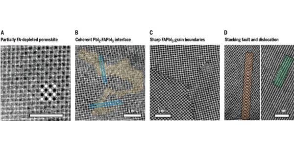
The team’s new technique enabled them to observe a completely new range of phenomena pertaining to hybrid perovskites, including important properties such as the exact makeup of the grain boundaries and other interfaces. Using the ePSIC (the Electron Physical Science Imaging Centre) E02 microscope and the ARM200 microscope at the Department of Materials, University of Oxford, the team developed a new technique which allowed them to image the hybrid photoactive perovskites thin films with atomic resolution. This gave them unprecedented insights into their atomic makeup and provided them with information that is invisible to every other technique.
The team observed a range of crystallographic defects that have never been considered for hybrid perovskites and which are known in other solar cell materials to be highly detrimental to the overall performance. Dr. Mathias Uller Rothmann, from the Department of Physics, University of Oxford explains; “This is the final step on the way to being able to image, and thus understand, these important solar cell materials at the most fundamental, atomic level. It is a significant discovery that has not been accomplished successfully before despite these materials being some of the most intensively studied in the world over the past 8 years. The material damages incredibly quickly under an electron beam, so we had to turn the electron dose down to the point where we were running at the limits of what the detectors can record.
The crucial role of a direct‐detection electron‐counting camera in reducing the required electron dose is outlined, which is indispensable for imaging extremely sensitive organic-inorganic hybrid perovskites. In fact, the damage happens so fast that under “normal” imaging conditions, the damage is done before you realise it. This means that there is probably a relatively large amount of literature out there which has made observations based on the damaged version of the material, and not the one that goes in the actual solar cells.”
Dr. Chris Allen, Principal Electron Microscopist at ePSIC says; “Imaging beam sensitive materials at atomic resolution is extremely challenging as the high energy electrons tend to damage the sample, altering its atomic structure. By adopting an imaging technique not usually associated with low electron dose imaging, this collaboration between scientists at the University of Oxford and ePSIC has achieved unprecedented resolution on this important class of materials. Not only has this answered questions about the atomic structure of hybrid perovskites but also opens avenues of research into many other beam sensitive materials.”
In addition to reviewing published works, the results of initial attempts to perform atomic‐resolution elemental mapping for an all‐inorganic HP and image a hybrid HP using scanning TEM are introduced. The paper reviews a combination of conditions that can now be used for imaging the materials as well as images of microscopic properties that have never been observed before in these materials. The team describes this as revolutionary because it now allows scientists to study exactly what the local makeup of the films is with atomic precision and accuracy. This technique is fairly widely used to study other materials, but due to the remarkably unstable nature of the photoactive perovskites, especially under an electron beam, this has not been possible for hybrid perovskites until now. Electron microscopy characterization of halide perovskite materials at the atomic resolution is difficult due to their extreme sensitivity to electron‐beam irradiation.
The team’s new technique enabled them to observe a completely new range of phenomena pertaining to hybrid perovskites, including important properties such as the exact makeup of the grain boundaries and other interfaces, which other techniques have not been able to resolve. Imaging conditions that are used to capture intact structures of various halide perovskites are summarized and analyzed, with the aim of providing guidance on this challenging subject. Additionally, the team observed a range of crystallographic defects that have never been considered for hybrid perovskites and which are known in other solar cell materials to be highly detrimental to the overall performance. Removing these defects will be important for high performance, but until now, it was impossible to reliably identify their presence.