Indium nitride (InN) is a semiconductor material with a tiny bandgap that has potential applications in solar cells and high-speed electronics. It has good electron transport capabilities, a low effective electron mass, and a surface electron accumulation layer, making it an ideal material for the manufacture of high-frequency devices such as high-electron mobility transistors.
The bandgap of InN has now been established as ~0.7 eV depending on temperature (the obsolete value is 1.97 eV). The effective electron mass has been recently determined by high magnetic field measurements, m* =0.055 m0. Alloyed with GaN, the ternary system InGaN has a direct bandgap span from the infrared (0.69 eV) to the ultraviolet (3.4 eV).
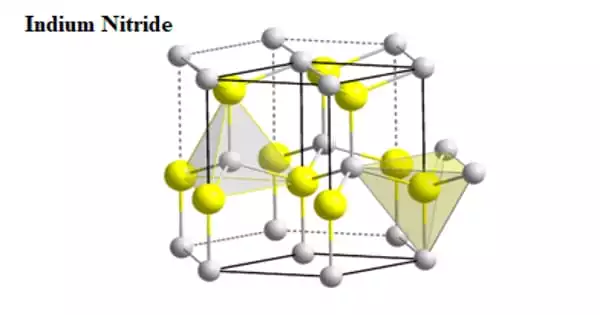
Properties
The thermal characteristics of InN were determined using single crystals of indium nitride produced using the nitrogen microwave plasma technique. The specific heat of InN was measured at temperatures ranging from 150 to 300 K. Due to the very low enthalpy of formation and the lack of an adequate substrate, growing a good quality epitaxial InN layer is a difficult operation.
- Crystal Structure: Wurtzite (hexagonal)
- Band Gap: 0.65 eV
- Molecular Weight: 128.83
- Melting Point: 1100 °C
- Density: 6.81 g cm-3
- Young’s Modulus: 308 GPa
- Bulk Modulus: 140 Gpa

Currently, research is being conducted to build solar cells using nitride-based semiconductors. An optical match to the solar spectrum can be accomplished by using one or more indium gallium nitride (InGaN) alloys. InN’s bandgap enables for the use of wavelengths as long as 1900 nm. However, many obstacles must be addressed before such solar cells may be commercialized: One of the most difficult issues is p-type doping of InN and indium-rich InGaN. It has been challenging to develop InN heteroepitaxially with other nitrides (GaN, AlN).
Metalorganic chemical vapour deposition can be used to create thin layers of InN. (MOCVD).
Superconductivity
At liquid helium temperatures, thin polycrystalline coatings of indium nitride can be very conductive and even superconductive. The superconducting transition temperature Tc varies from 0 K to around 3 K depending on the film structure and carrier density of each sample. Tc can reach 3.97 K with magnesium doping. Superconductivity endures in the presence of strong magnetic fields (a few teslas), as opposed to superconductivity in In metal, which is quenched by fields of only 0.03 tesla. Nonetheless, according to the Ginzburg–Landau theory, superconductivity is attributed to metallic indium chains or nanoclusters, where the small size increases the critical magnetic field.
Applications
Currently, research is being conducted to build solar cells using nitride-based semiconductors. The alloy indium gallium nitride is used to provide an optical match to the solar spectrum. If these solar cells are to become a commercial reality, p-type doping of indium nitride and indium rich indium gallium nitride must be overcome.
Safety Information
Indium nitride may cause skin and eye irritation, however there are no documented sensitizing effects. Indium compounds can induce joint and bone pain, teeth decay, neurological and gastrointestinal issues, heart pain, and general debility. Experiments on animals also show that indium can induce decreased food and water consumption, weight loss, pulmonary edema, pneumonia, blood, liver, and kidney damage, leg paralysis, and harm to the brain, heart, adrenals, and spleen. The acute and chronic toxicity of this drug is unknown.