Indium aluminum nitride (InAlN) is a ternary semiconductor material that is a combination of indium nitride (InN) and aluminum nitride (AlN). It belongs to the III-nitride family of materials, which are widely used in the development of electronic and optoelectronic devices, such as LEDs, lasers, and high-power transistors.
It is a semiconductor material with a direct bandgap that is used in the fabrication of electronic and photonic devices. It is an alloy of indium nitride and aluminum nitride that belongs to the III-V group of semiconductors and is closely related to the more commonly used gallium nitride. Because of its large direct bandgap and ability to operate at temperatures of up to 1000 °C, it is particularly appealing in applications requiring high stability and reliability, such as the space industry. InAlN high-electron-mobility transistors (HEMTs) are appealing candidates for such applications due to their ability to lattice-match to gallium nitride, thereby eliminating a previously reported failure route in the closely related aluminium gallium nitride HEMTs.
InAlN has unique properties that make it attractive for various applications. For example, it has a wide bandgap and a high electron mobility, which makes it suitable for high-frequency and high-power electronics. It also has good thermal stability and chemical resistance, which are important for device reliability and durability.
Properties
- Bandgap: InAlN has a wide bandgap of around 2.0 to 3.5 electron volts (eV), depending on its composition. This makes it suitable for high-power and high-frequency electronic devices.
- Crystal structure: InAlN has a wurtzite crystal structure, similar to that of gallium nitride (GaN) and aluminum nitride (AlN).
- Thermal stability: InAlN has high thermal stability and can withstand high temperatures, making it useful for high-temperature electronic and optoelectronic devices.
- High electron mobility: InAlN has high electron mobility, making it suitable for high-speed electronic devices such as high-electron mobility transistors (HEMTs).
- Low dislocation density: InAlN has low dislocation density, which helps to reduce defects in electronic devices and improve their performance.
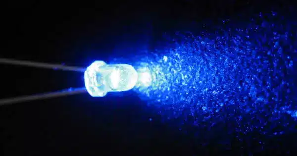
- Optical properties: InAlN has strong absorption in the ultraviolet (UV) region, making it useful for UV photodetectors and light-emitting diodes (LEDs).
InAlN is grown epitaxially in combination with other semiconductor materials such as gallium nitride, aluminum nitride, and their associated alloys to produce semiconductor wafers, which are then used as the active component in semiconductor device fabrication. Due to the widely different properties of aluminium nitride and indium nitride, InAlN is an especially difficult material to grow epitaxially, and the resulting narrow window for optimized growth can lead to contamination (i.e. to produce indium gallium aluminium nitride) and poor crystal quality, at least when compared to AlGaN. Similarly, device fabrication techniques optimized for AlGaN devices may need to be tweaked to account for InAlN’s different material properties.
InAlN can be grown using various methods, such as metal-organic chemical vapor deposition (MOCVD) and molecular beam epitaxy (MBE). The growth conditions can be tuned to control the material properties and achieve the desired device performance.
Overall, InAlN is a promising material for advanced electronic and optoelectronic applications, and research is ongoing to explore its potential in various fields.