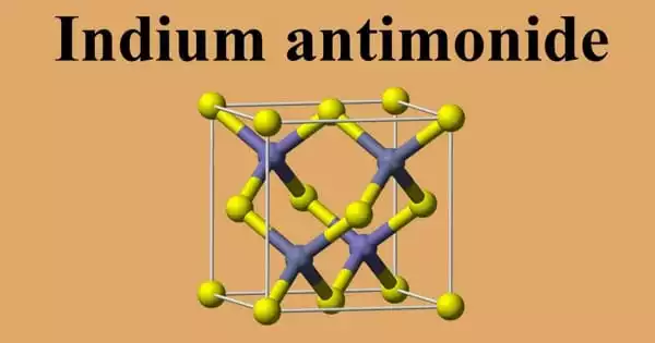
Indium antimonide (InSb) is a crystalline chemical composed of indium (In) and antimony (Sb) (Sb). It is a semiconducting and photosensitive material made from the synthetic compound InSb of indium and antimony that is utilized mostly in infrared photodetectors. It is a III-V semiconductor material with a low band gap that is utilized in infrared detectors such as thermal imaging cameras, FLIR systems, infrared homing missile guidance systems, and infrared astronomy. The indium antimonide detectors have a wavelength range of 1–5 m.
Indium antimonide was a common detector in single-detector mechanically scanned thermal imaging systems in the past. Because it is a strong photo-Dember emitter, it can also be used as a terahertz radiation source.
Physical properties
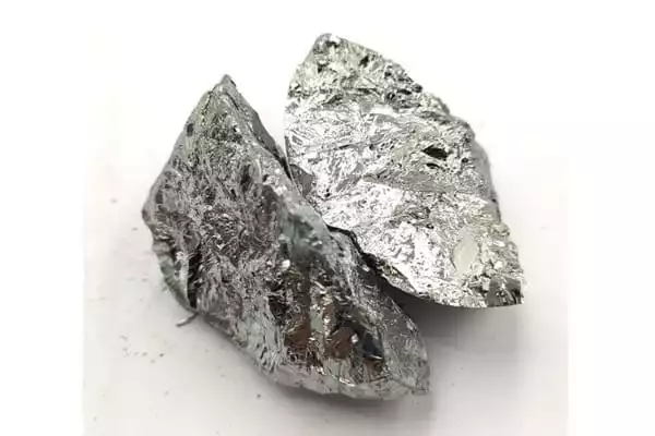
InSb appears as dark-grey silvery metal particles or powder with a vitreous luster. When heated over 500 °C, it melts and decomposes, releasing antimony and antimony oxide fumes. The crystal structure is zincblende, with a lattice constant of 0.648 nm.
- Molecular Weight: 236.58
- Appearance: Dark grey metallic crystals
- Melting Point: 527 °C
- Boiling Point: N/A
- Density: 5.78 g/cm3
- Solubility in H2O: Insoluble
Electronic properties
InSb is a semiconductor with a narrow band gap with an energy band gap of 0.17 eV at 300 K and 0.23 eV at 80 K. Except for carbon nanotubes, undoped InSb has the highest ambient-temperature electron mobility (78000 cm2/Vs), electron drift velocity, and ballistic length (up to 0.7 m at 300 K) of any known semiconductor.
When exposed to infrared radiation, indium antimonide photodiode detectors generate an electric current. The internal quantum efficiency of InSb is effectively 100 percent, however it varies with thickness, especially for near bandedge photons. InSb detectors, like any narrow bandgap materials, require periodic recalibrations, which adds to the imaging system’s complexity. Where great sensitivity is required, such as in long-range military thermal imaging systems, the increased complexity is worthwhile. InSb detectors, which must operate at cryogenic temperatures, also require cooling (typically 80 K). There are large arrays (up to 20482048 pixels) available. HgCdTe and PtSi are two materials with similar applications.
History
Liu and Peretti described the intermetallic compound for the first time in 1951, providing information on its homogeneity range, structure type, and lattice constant. Heinrich Welker created polycrystalline ingots of InSb in 1952, however they were not very pure by today’s semiconductor standards. Welker was intrigued by the semiconducting features of III-V compounds and wanted to investigate them thoroughly. He noticed that InSb had a tiny direct band gap and a strong electron mobility. Slow cooling from liquid melt has been used to create InSb crystals since at least 1954.