
Researchers have created a highly accurate method for assembling multiple micron-scale optical devices that are extremely close together on a single chip. The new approach may one day enable high-volume production of chip-based optical systems, allowing for more compact optical communications devices and advanced imagers.
“The evolution of electronics based on silicon transistors has enabled increasingly powerful and flexible systems on a chip,” says Dimitars Jevtics of the University of Strathclyde in the United Kingdom. “Optical systems on a chip, on the other hand, require the integration of different materials on a single chip and, as a result, have not seen the same scale development as silicon electronics.”
Jevtics and colleagues describe their new transfer printing process and demonstrate its ability to place devices made of multiple materials on a single chip, all integrated within a footprint similar in size to the devices themselves in the Optica Publishing Group journal Optical Materials Express. Unlike other methods, which are typically limited to a single material, this new method provides a toolbox of materials from which future system designers can draw.
Researchers describe a highly accurate way to assemble multiple micron-scale optical devices extremely close together on a single chip. The approach could allow high-volume manufacturing of chip-based optical systems that would enable more compact optical communications devices and advanced imagers.
“On-chip optical communications, for example, will necessitate the integration of optical sources, channels, and detectors onto sub-assemblies that can be integrated with silicon chips,” Jevtics explained. “Our transfer printing method could be scaled up to accommodate thousands of devices made from various materials on a single wafer. Micron-scale optical devices could then be integrated into future computer chips for high-density communications or lab-on-a-chip bio-sensing platforms.”
A better way to pick and place
One of the most difficult aspects of assembling multiple devices on a chip is attempting to place them very close together without disturbing devices already on the chip. To accomplish this, the researchers devised a reversible adhesion method in which a device is picked up and released from its growth substrate before being placed on a new surface.
The new method picks up an optical device from the substrate using a soft polymer stamp mounted on a robotic motion control stage. The substrate to be placed is then positioned beneath the suspended device and precisely aligned using a microscope. When the two surfaces are properly aligned, the device is released from the polymer stamp and deposited onto the target surface. This approach was made possible by advancements in precise micro-assembly robotics, nanofabrication techniques, and microscopy image processing.
“We can engineer whether a device will be picked up or released by carefully designing the geometry of the stamp to match the device and controlling the stickiness of the polymer material,” said Jevtics. “When optimized, this process causes no damage and can be scaled up to be compatible with wafer-scale manufacturing.”
Creating a densely packed chip
To demonstrate the new technique, the researchers combined optical resonators made of aluminum gallium arsenide, diamond, and gallium nitride onto a single chip. These optical resonators demonstrated good optical transmission, indicating that the integration was successful.
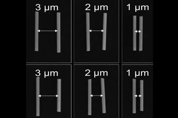
They also used the printing method to create semiconductor nanowire lasers by placing nanowires in spatially dense arrangements on host surfaces. Scanning electronic microscopy measurements of the distance between the nanowires revealed a spatial accuracy of 100 nanometers. They were able to create a multi-wavelength nanolaser system by placing semiconductor nanowires on silicon dioxide.
“This printing approach is not limited to optical devices as a manufacturing technique,” said Jevtics. “We hope that electronics specialists will see opportunities for it to be used in future systems.”
The researchers are now working to replicate these findings with a larger number of devices to demonstrate that it works at a larger scale. They also intend to combine their transfer printing approach with a previously developed automated alignment technique to enable rapid measurement, selection, and transfer of hundreds of isolated devices for applications in imaging and hybrid optical circuits.